
Engineering Services
End-to-end design, layout, verification, and manufacturing services for the Indian semiconductor and ESDM industry — backed by 30+ years of combined expertise.
What We Offer
Our Service Portfolio
Four complementary service domains spanning the entire semiconductor and electronics design lifecycle.
ASIC Layout
Analog, full custom, and standard cell layout services with dedicated team options.
Learn moreAnalog IP Design
ADCs, DACs, PLLs, PMICs, ROICs, and RF/Microwave blocks — full mixed-signal IP catalog.
Learn moreFPGA Services
RTL design, FPGA realization, ASIC migration, and SV-UVM verification expertise.
Learn morePCB Design
Schematic to manufacturing — high-speed routing, SI/PI analysis, assembly, and testing.
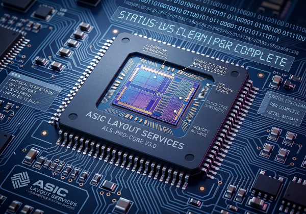
Learn moreASIC Layout Services
Comprehensive ASIC layout support backed by an experienced team of layout engineers and a structured training and onboarding program. We deliver complex semiconductor layouts under rigorous Intellectual Property protection protocols and seamless customer collaboration.
Our flexible engagement models accommodate every project scope — from quick offsite tasks to multi-year dedicated teams.
Design Types Covered
Analog Design
Specialized layout for analog circuits with attention to matching, parasitics, and noise sensitivity.
Full Custom Design
Complete custom layout implementation for performance-critical and area-optimized blocks.
Standard Cell Design
Standard-cell-based digital layout solutions for SoC and ASIC implementations.
Engagement Models
Dedicated Offsite Team
Long-term dedicated layout team operating from our Hyderabad office with strict IP protocols.
Project-Specific Team
Remote layout support tailored to specific project scope, also managed from Hyderabad.
Onsite Resources
Layout engineers deployed at customer locations across India for medium to long-term engagements.
Analog IP Design Services
Specialized analog and mixed-signal IP design covering data conversion, power management, imaging readout, RF/microwave, and SoC interface optimization. Our team builds production-ready IP blocks tailored to your process node and application.

Analog / Mixed Signal
Data conversion and timing IPs for complex SoCs.
Power Management IC (PMIC)
Power regulation solutions addressing efficiency and distribution challenges.
Readout IC (ROIC)
Infrared imaging readout for thermal and sensor applications.
SoC Interface Solutions
Optimize SoC integration for power, area, and performance — streamlining system-on-chip implementations.
RF / Microwave
High-performance RFIC building blocks and complete radio systems using industry-standard protocols.
FPGA Services
Comprehensive FPGA design and verification services — from RTL development to ASIC migration. Our verification team employs modern methodologies to handle complex SoC and IP designs from scratch.
Services are typically executed from our India facility with flexibility for onsite customer-location support when needed.
FPGA Realization
Design of RTL targeted at FPGAs, FPGA system design, and migration support from FPGA to ASIC for production volumes.
- RTL design and architecture
- FPGA system integration
- FPGA-to-ASIC migration support
FPGA / ASIC Verification
Comprehensive verification services using modern methodologies and experienced engineers — from component-level work to complete SoC verification.
- Complete SoC and IP verification from scratch
- Component-level and lifecycle implementations
Verification Methodologies
Formal verification methods
SystemVerilog Universal Verification Methodology
Property Specification Language
Hardware-in-the-loop validation
PCB Design Services
End-to-end PCB design covering the complete development lifecycle — from initial schematic review through manufacturing, assembly, and validation. Standards-compliant deliverables with deep expertise in high-speed interfaces.
Our team handles complex multilayer designs balancing signal integrity, power distribution, and thermal management.
Complete PCB Design Workflow
Schematic Review
Detailed analysis of customer-approved schematics, including obsolescence checks, critical signal review (clocks, high-speed lines), and differential pair verification.
Library Creation
Footprint development per IPC 7351 standards and manufacturer datasheet recommendations, with version-controlled libraries.
Pre-Layout SI Analysis
Routing constraints and stack-up validation for high-speed interfaces — DDR3, Flash, Ethernet (SGMII/RGMII), PCI Express.
PCB Layout Design
Board outline, DFM/DFA placement, IPC 2221 routing, design rule and database checks, and Gerber RS 274-X output.
Post-Layout SI/PI
S-parameter extraction via 3D EM, 2D trace analysis, and power integrity validation before sign-off.
Thermal Analysis
Temperature profiling and cooling requirement assessment for FPGA, voltage regulator modules, and other critical components.
PCB Manufacturing
RoHS-compliant production per IPC 6012 Class 2. Deliverables: Gerbers, fabrication drawings, Excellon drill files, manufacturing notes.
PCB Assembly
RoHS-verified BOM procurement, IPC-A-610 Class 2 assembly, pick-and-place files, and BGA/LGA X-Ray inspection on request.
Testing & Validation
Visual, ICT, power-on, JTAG, DDR3 memory, FPGA interface, and 1000Base-X SGMII testing for full reliability validation.
High-Speed Interfaces
Standards Compliance
Why Craftronics
Engineered for Trust
Why customers across Defense, Space, Industrial, Research, and Education choose us for their semiconductor and electronics design needs.
Intellectual Property Protection
Established protocols safeguarding your designs, IP blocks, and confidential data across every engagement.
30+ Years Combined
Deep techno-commercial expertise across Defense, Space, and Semiconductor sectors.
Flexible Engagement
Onsite, offsite, dedicated, or project-specific — we adapt to your needs.
Best-in-Class Tools
Cadence, Dassault Systemes, and Mirabilis Design platforms in-house.

Have a Project in Mind?
Let's discuss your requirements. Whether you need a dedicated team or a quick design review, our engineers are ready to help.